 Technology Limited")
Packaging technology is more important than chip technology in Mini LED technology
2023-05-10(3608)Browse
Making Mini LED display panel products involves various comprehensive technologies such as LED chips, packaging, PCB board design and manufacturing, materials, equipment, testing, repair, production process, driver IC, control sending/receiving, power supply, energy-saving, box splicing, consistency correction, panel protection, etc. Among them, LED chip technology and LED chip packaging technology are the two most important underlying support technologies. Therefore, other comprehensive technologies are related to chips What kind of symbiotic relationship is packaging technology? This article will discuss this topic to give everyone a general overview of the key points of Mini LED technology, so as not to get lost or mysterious when hearing about Mini LED technology.
The concept of Mini LED technology has different contexts and meanings in different industries. For example, in the LCD industry, Mini LED often refers to backlight panel technology. A straight down backlight panel with a 5mm bead spacing can be called Mini LED technology. But in the LED display industry, this is unimaginable because a 5mm pixel spacing cannot even be considered small spacing technology. So the issue we are discussing today is limited to the LED display field, and the pixel spacing is within the range of 1.5mm-0.3mm in Mini LED technology. But the discussion here also has certain reference value for the backlight panel technology in the LCD industry.
1、 Chip Technology of Mini LED
LED chip technology has transitioned from the formal era to the flip chip era, and the application of flip chip is the trend. The size of LED chips is also standardized between 50 and 200? Between m. At present, in the range of 1.5-1.2mm pixel spacing, legitimate chips can also be used. In the range of 1.2-0.7mm pixel spacing, there are solutions for using legitimate chips for red light and inverted chips for blue-green light. In the range of 0.7-0.3mm pixel spacing, RGB still needs to use flip chips. Therefore, Mini LED products can be divided into regular chips and flip chips.
The advantages of using flip chip technology on Mini LED products are that it can improve brightness, save more power, have better contrast, require less equipment investment, and achieve higher production efficiency. It can also achieve smaller physical pixel space layout and effectively improve the internal failure problem of display panel pixels.
So, as the pixel spacing moves towards a smaller target of 0.3mm, the forward chip technology will fully transition to the flip chip technology.
2、 Packaging Technology of Mini LED
With the development of LED chip technology, LED packaging technology has also made innovations and breakthroughs in theory and process practice, transitioning from the era of bracket based packaging light driver separation technology to the era of integrated packaging light driver integration technology without brackets. In the process of packaging technology evolution, a temporary bracket type limited integrated packaging light drive separation technology has also emerged.
In the classification of lamp drive separation technology in bracket packaging, we know that there are DIP technology and SMD technology. But for Mini LED display products, only SMD technology can achieve a relatively stable pixel spacing between 1.2 and 1.5mm. However, facing the panel level pixel loss rate and full screen pixel loss rate required by the million level indicator of Mini LED display products, this technology may feel inadequate. When manufacturing display products with pixel spacing below P1.2, it encounters many insurmountable technical bottlenecks and gradually loses its market advantage.
The separation technology of bracket based limited integrated packaging light driver is a transitional packaging technology that emerged after the bracket based packaging technology and the non bracket based integrated packaging technology in terms of time. In this type of technology classification, we currently see 2 in 1 packaging technology, 4 in 1 packaging technology, and N in 1 (IMD) packaging technology. They not only want to draw on the integration concept of COBIP (COB integrated packaging), but also do not want to give up the simplicity of SMD bracket packaging technology, so it has been difficult for their products to undergo radical changes. This technology is essentially a hybrid packaging technology of SMD and COBIP, which mostly inherits the genes of SMD and only introduces COB packaging elements and integration ideas, hence it is also known as COBLIP (Chip On Board Limited Integrated Packaging) technology. Due to the lack of effective measures to reduce bracket pins, it still belongs to the category of bracket type packaging light drive separation technology, and cannot fundamentally solve the problem of pixel out of pixel failure caused by bracket pins. Although there is an optimization and improvement plan to reduce the number of bracket pins, the effect of this effort is not obvious, and it cannot truly overcome the fact that the panel level pixel loss rate and the low order ability of the full screen pixel rate of 10000 or 100000 levels. In the 1.2-0.9mm pixel range of Mini LED, it will encounter the same technical bottleneck as SMD packaging technology.
In addition, from the perspective of industrial technology upgrading, future 4K and 8K ultra high definition video display products and Mini LED display products will definitely require high-end panel level million level display products. And this transitional technology, although packaging companies in the industry chain can achieve device level of one million, downstream enterprises using this million level device to achieve panel level will become 100000 level products, which is actually a waste of industrial resources and a serious industrial problem that should be taken seriously by the entire industry.
New Information
-
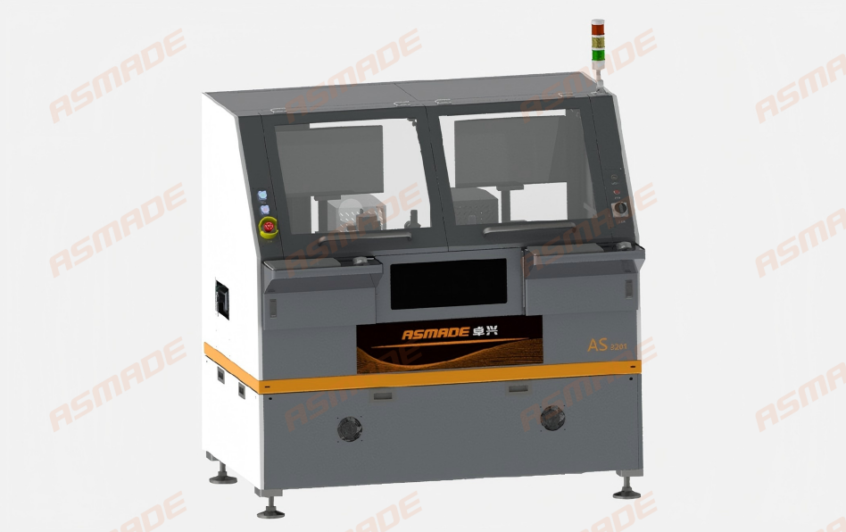
AS3201 Bulk Component Mounter: Supporting LED Beads and Bulk Component Mounting at Any Pitch, and Improving Quick Changeover Efficiency
lEquipping dual vibrationfeeding, andsupporting0606–2121 LE...
-
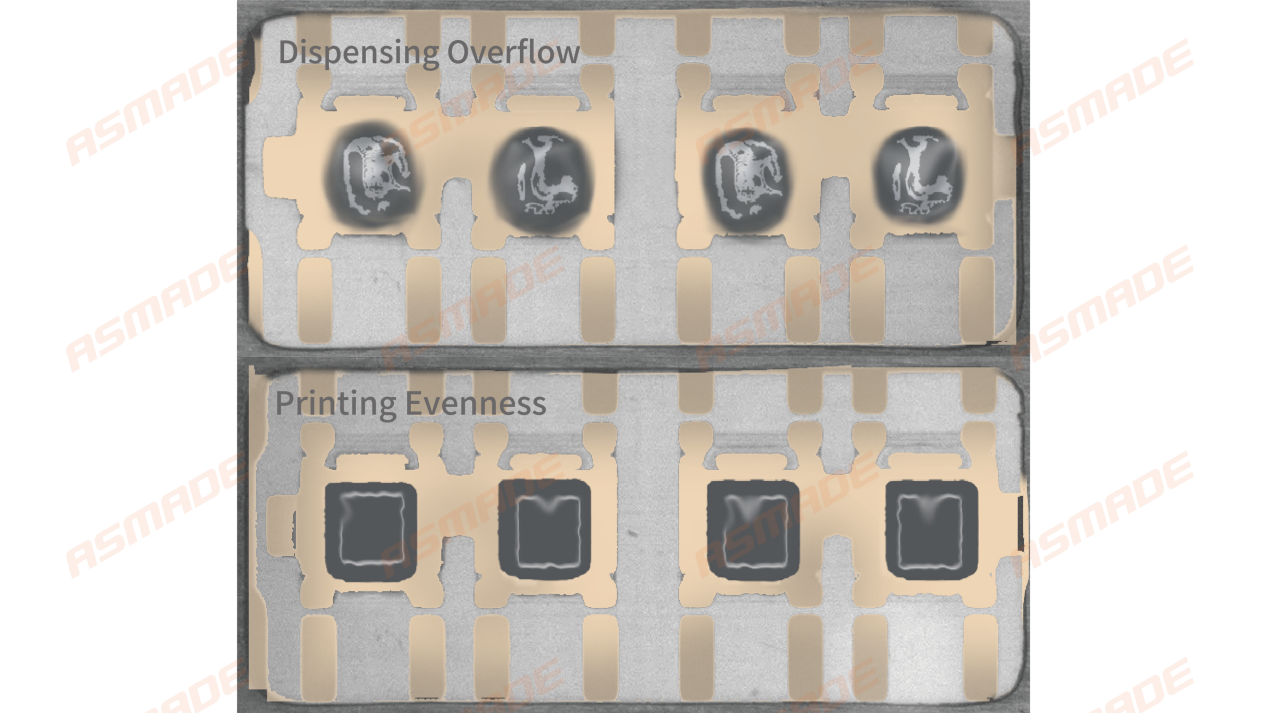
On-Chip Printing | Effectively Solving Dispensing and Printing Issues in Power Device Packaging
In theclip bonding packagingprocess of power devices, dispen...
-
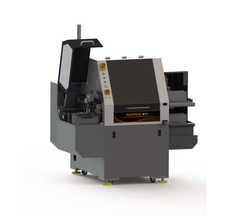
Chip-Level Printer | Printing power device frames in the X axis direction, combined with on-chip printing technology
The world's first semiconductor chip-level printer with ...
-
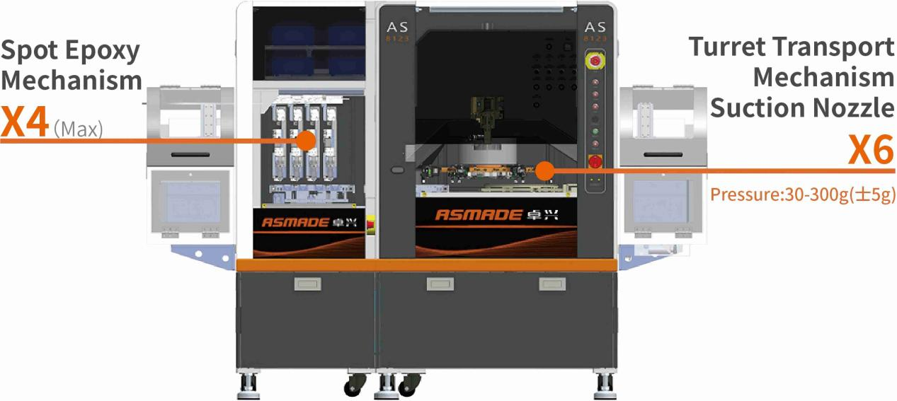
Semiconductor Epoxy Die Bonder | Combining Spot Epoxy Process with Die Bonding Process in One Machine, Capable of Handling Numerous Products.
The Epoxy Die Bonder is a semiconductor machine that feature...
0755-29691921
Hotline:0755-29691921
Phone:0755-29691921
Fax:0755-29691921
Email:market@asmade.cn
Address:Building 3, Xifengcheng Industrial Park, Fuhai Street, Bao'an District, Shenzhen City, Guangdong Province


 0755-29691921