 Technology Limited")
Asmade Semiconductor 3C Solid Crystal Rule: a new technological revolution that leverages the LED display industry
2023-05-10(3422)Browse
This year's National Two Sessions proposed to promote the deep integration of technological innovation and the real economy, better play the role of innovation-driven development, and encourage enterprises to promote industry development through technological innovation. Especially in the manufacturing industry, the "14th Five-Year Plan" and "2035 Long-term Goals" clearly mentioned planning suggestions on promoting the integration and development of new technologies and manufacturing industries, and supported the use of new technologies to promote the development and upgrading of manufacturing industries. New technology creates a new era. As the overall solution service provider of Mini LED packaging process, Zhuoxing Semiconductor keeps up with the trend of the times and creatively develops 3C die-bonding rules to provide solutions for the packaging process technical problems that need to be solved urgently for the development and upgrading of LEDs to Mini LEDs. plan.

Showing the complexity and sophistication of the industry in terms of intelligent upgrades, technology companies with full-dimensional technology and years of practical experience are required to provide solutions. Zhuoxing Semiconductor has assumed such a role. Conduct special research on the technical and process problems faced by Mini LED die-bonding, inspection, bonding and rework processes, especially the problems of how to be more accurate, faster, larger and more efficient in the packaging process of Mini LED key links, Zhuoxing Semiconductor took the lead in proposing 3C die-bonding rules, namely: Correction angle correction, Control pressure control, and Continuity continuous die-bonding.

This is the first time in the industry that a company has proposed a methodology to systematically solve the problem of Mini LED die bonding. Zhuoxing Semiconductor, which focuses on the research and development and manufacture of high-precision semiconductor equipment, has more than 20 invention patents. With its solid semiconductor manufacturing background and technical advantages, it has brought a new "problem-solving idea" to the Mini LED industry.

3C Die Bonding Rule 1: Correction Angle Correction
Zhuoxing Semiconductor’s innovative swing arm wafer dynamic correction design improves the accuracy of wafer welding through small-angle and small-scale optimization adjustments. The position error is ±15um, and the angle error is less than 1 degree, so as to meet the LED small-pitch technical standard: 0.6-1.25 mm, which solves the problem of the very critical die-bonding pitch for Mini LEDs.
The angle correction advocated by Zhuoxing Semiconductor consists of two parts: the first is the correction of the wafer ring, which ensures that the position of the swing arm of the die bonder is more accurate when grabbing the wafer, and the grabbing success rate is higher; the second is the correction of the wafer. After the wafer is grasped, the dynamic angle is adjusted to ensure that the wafer fit posture is corrected and the position error is smaller. Through the two-level, two-step die-bonding dynamic correction, the chip bonding position is ensured to be more accurate, so that the chip pitch can be smaller, making Mini LED or even Micro LED possible.
3C Die Bonding Rule 2: Control Pressure Control
Solving the problem of chip spacing is only the first step in the long march of LED. If you want to apply Mini LED in a wide range and large size, such as TVs, computer monitors, and outdoor large-scale smart displays, the display substrate must be made larger while meeting the small-pitch bonding of chips. Another problem arises with larger substrates, warping and unevenness naturally occurring as the area increases. If the bonding module of the traditional die bonder does not carry out pressure control, it will lead to inconsistent chip bonding and lower yield rate, thus failing to meet the 99.99% standard required by Mini LED.
Therefore, the key to the above problems is the pressure control of the bonding module. Zhuoxing semiconductor die bonder equipment innovates the pressure control of die bond operation - the bonding module has built-in high-precision linear and rotary motions, and performs pressure detection and control while the chips are bonded to ensure that each chip can be used with perfect strength Attached to the corresponding position of the substrate, the yield rate of die bonding can reach more than 99.99%. Regardless of the large-size substrate warpage problem, the substrate can be made larger (substrate width ≥ 200mm), Zhuoxing Semiconductor’s 3C die-bonding method “escorts” the large-size substrate die-bonding.
3C Die Bonding Rule 3: Continuity Continuous Die Bonding
The large-size substrate realizes the soft landing of the chip through pressure control and ensures the yield rate of die bonding, so how to ensure the efficiency of die bonding? Because the solder paste for attaching chips is time-sensitive, when the solder paste is denatured, it will not be able to attach the chip normally, so the die must be pasted before the denaturation of the solder paste, and the more the number of dies, the higher the display clarity. The display size is also larger.
Zhuoxing Semiconductor's 3C die-bonding method solves the problem of efficiency through "continuous die-bonding". Zhuoxing Semiconductor innovates the dual-arm synchronous die bonding mode, which doubles the efficiency of traditional die bonding machines per unit time. In addition, Zhuo Xing Semiconductor also has a dual-arm 6-wafer ring mixed design, which can complete RGB three-color die bonding in one clamping, with higher efficiency and more die bonding per unit time. At present, Zhuoxing Semiconductor's die bonding efficiency can reach 40K/H, which is higher than the market average.

Upgrading the manufacturing industry is not only a corporate responsibility, but also a social mission. Obviously, Zhuo Xing Semiconductor has done a good job in both! Through the 3C crystal bonding method, a technological innovation and upgrade of the entire LED display industry is carried out, especially for the key link of LED - the packaging process, Zhuoxing Semiconductor first proposed a systematic overall solution, which provides a realizable solution for the large-scale application of Mini LED path of. Technological innovation, industry upgrading, Zhuoxing Semiconductor continues to practice its original intention of "prospering national semiconductor equipment, breaking foreign technology blockade", helping the transformation and upgrading of the semiconductor industry and even the entire Chinese manufacturing industry!
New Information
-
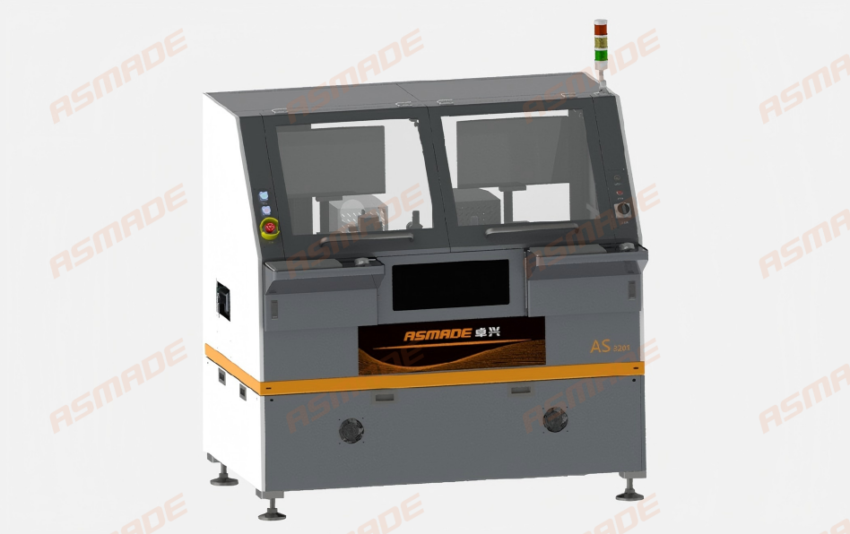
AS3201 Bulk Component Mounter: Supporting LED Beads and Bulk Component Mounting at Any Pitch, and Improving Quick Changeover Efficiency
lEquipping dual vibrationfeeding, andsupporting0606–2121 LE...
-
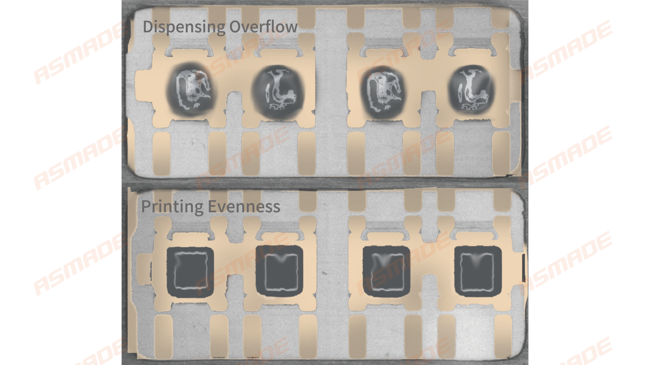
On-Chip Printing | Effectively Solving Dispensing and Printing Issues in Power Device Packaging
In theclip bonding packagingprocess of power devices, dispen...
-
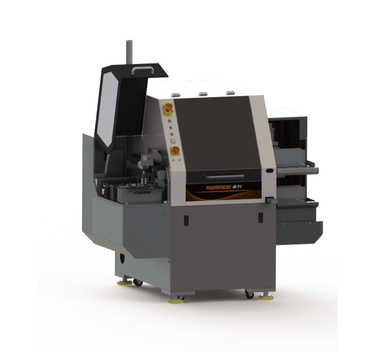
Chip-Level Printer | Printing power device frames in the X axis direction, combined with on-chip printing technology
The world's first semiconductor chip-level printer with ...
-
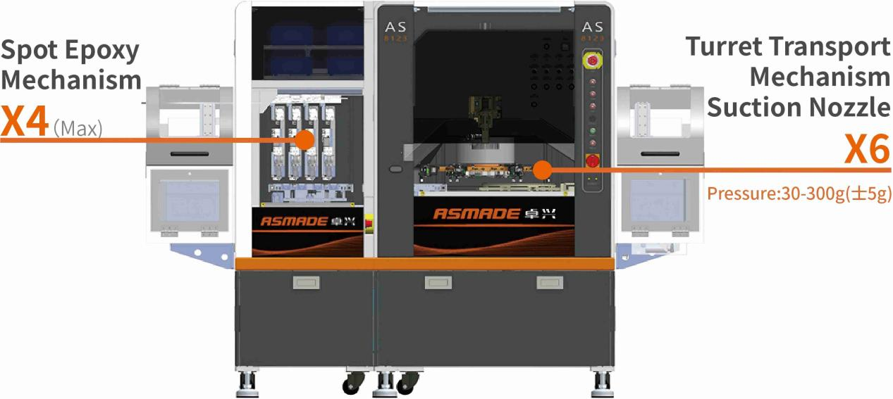
Semiconductor Epoxy Die Bonder | Combining Spot Epoxy Process with Die Bonding Process in One Machine, Capable of Handling Numerous Products.
The Epoxy Die Bonder is a semiconductor machine that feature...
0755-29691921
Hotline:0755-29691921
Phone:0755-29691921
Fax:0755-29691921
Email:market@asmade.cn
Address:Building 3, Xifengcheng Industrial Park, Fuhai Street, Bao'an District, Shenzhen City, Guangdong Province


 0755-29691921